Press Release
Driving Fine Patterning and High Throughput in Maskless Lithography for Advanced Semiconductor Packaging
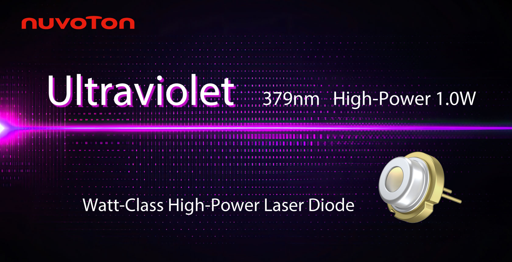
Nuvoton Releases High-Power Ultraviolet Laser Diode (379 nm, 1.0 W)
January 16, 2026
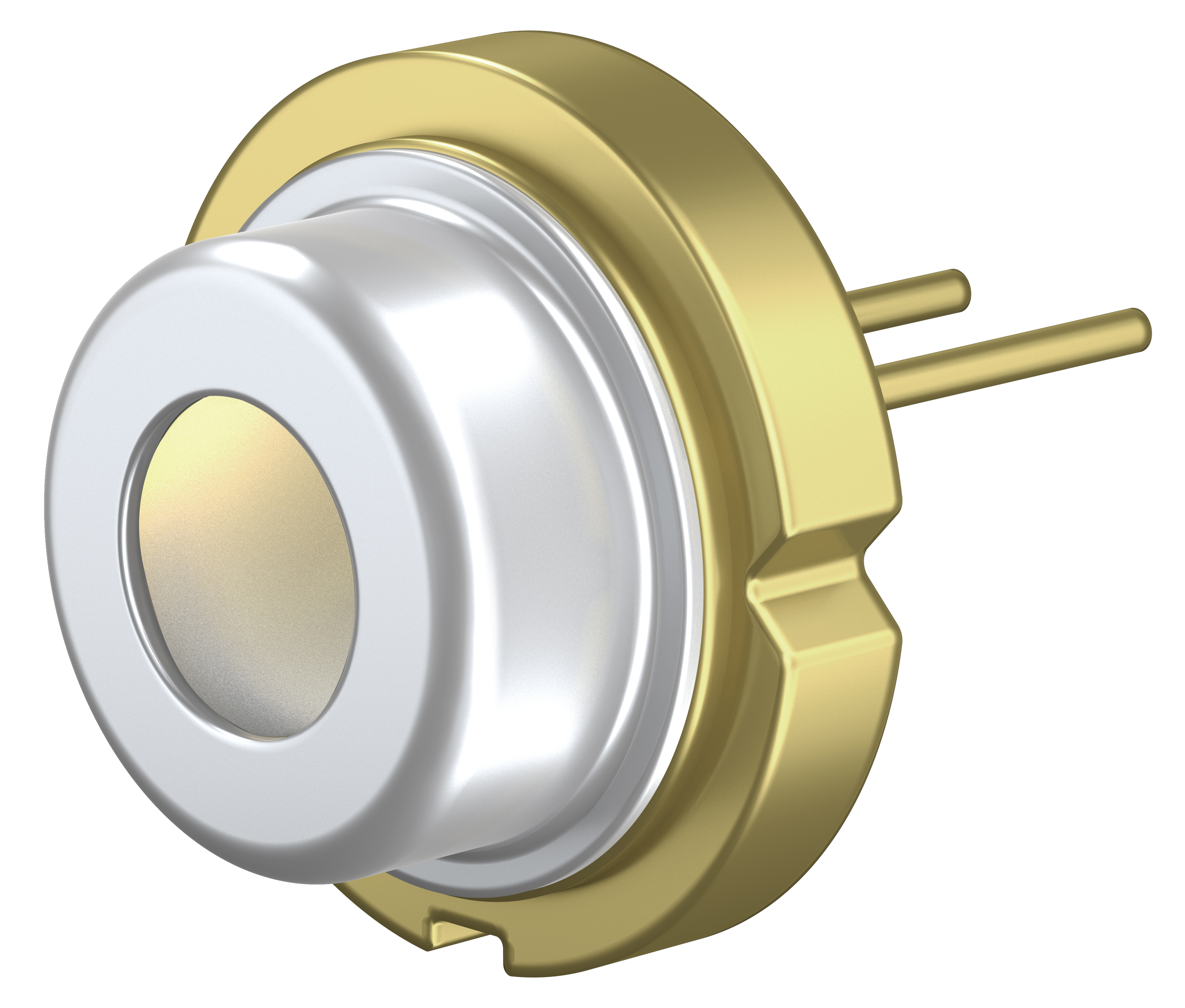
Kyoto, Japan, January 16, 2026 – Nuvoton Technology announced today the start of mass production of its high-power ultraviolet semiconductor laser (379 nm, 1.0 W)[1], which delivers industry-leading(*) optical output in a 9.0 mm diameter CAN package (TO-9)[2]. This product achieves short wavelength, high output power, and long lifetime—three elements previously considered difficult for ultraviolet semiconductor lasers—through our proprietary device structure and advanced high-heat-dissipation packaging technology. As a result, it contributes to fine patterning and improved production throughput in maskless lithography[3] for advanced semiconductor packaging[4].
(*)As of January 16, 2026, based on our research of semiconductor lasers emitting at 379 nm in a TO-9 CAN package under continuous-wave (CW) operation at a case temperature (Tc) of 25°C.
Achievements
- Achieves 1.0 W-class optical output at 379 nm, contributing to fine patterning and improved production throughput in maskless lithography for advanced semiconductor packaging.
- Improves heat dissipation of ultraviolet semiconductor lasers through our proprietary device structure and packaging technology, suppressing device degradation from self-heat generation and ultraviolet light and contributing to the extended lifetime of optical equipment.
- Expands the lineup of mercury lamp replacement solutions[5], enhancing flexibility in product selection to suit different applications.
・For more product details, please see here
Features of New Product
- Achieves 1.0 W-class optical output at 379 nm, contributing to fine patterning and improved production throughput in maskless lithography for advanced semiconductor packaging.
- Improves heat dissipation of ultraviolet semiconductor lasers through our proprietary device structure and packaging technology, suppressing device degradation from self-heat generation and ultraviolet light and contributing to the extended lifetime of optical equipment.
- Device structure to enhance wall-plug efficiency
- High thermal conduction package technology that efficiently dissipates heat
- Expands the lineup of mercury lamp replacement solutions, enhancing flexibility in product selection to suit different applications.
As demand grows for information processing capabilities driven by the evolution of artificial intelligence (AI), there is increasing need for higher performance from semiconductors than ever before. On the other hand, as the miniaturization of transistors approaches its physical and economic limits, semiconductor back-end package technologies and advanced semiconductor packaging, which allow for integration by arranging multiple semiconductor chips side by side or stacking them vertically, have been attracting attention.
In advanced semiconductor packaging, the mainstream method for forming wiring connections between multiple semiconductor chips has been exposure technology using the i-line (365 nm) of the mercury spectrum and photomasks (master masks of circuits). On the other hand, there has been growing interest in recent years in maskless lithography technology, which directly exposes (draws) wiring patterns based on design data without using photomasks.
This technology is considered to reduce the time and cost associated with the design and production of photomasks. Furthermore, because it is possible to directly imprint wiring patterns to match the surface shape of the target for drawing, alignment and correction are easier, and application to advanced semiconductor packages is currently under consideration.
As one of the key light sources in maskless lithography, semiconductor lasers have faced increasing demands for shorter wavelengths closer to the i-line (365 nm) and higher output, in order to enable finer wiring and improve equipment throughput. To meet these requirements, we have leveraged over 40 years of experience in laser design and manufacturing to develop and commercialize an ultraviolet semiconductor laser with a wavelength of 379 nm and an output of 1.0 W.
Ultraviolet semiconductor lasers generally suffer from significant heat generation caused by low wall-plug efficiency (WPE)[6], and a tendency for device degradation caused by ultraviolet light, making stable operation at high output levels above 1.0 W difficult to achieve. To address this, we took a dual approach by focusing on both a “device structure that enhances wall-plug efficiency (WPE)” and a “high thermal conduction package technology that effectively dissipates heat,” enabling us to develop a product that successfully combines short wavelength, high output, and long lifetime: a 1.0 W ultraviolet (379 nm) device. As a result, we are contributing to extending the lifetime of optical devices that utilize ultraviolet light.
In addition to optimizing the emission layer and optical guide layer, we have adopted a proprietary structure that precisely controls the doping profile. By reducing light absorption loss and operating voltage, this allows electrical energy to be converted into light more efficiently.
In addition to adopting a submount made of high thermal conductivity materials, the package materials have been revised to reduce thermal resistance. As a result, rises in device temperature are suppressed, allowing for stable operation at high output.
This product has been newly added to our lineup of "semiconductor laser-based alternatives to mercury lamps," providing customers with a new choice. With this addition, customers can flexibly select products according to application, installation environment, and required performance, thereby increasing the freedom of system design.
Details of this new product will be showcased at our booth at SPIE Photonics West 2026 in San Francisco, USA, and at OPIE’26 in Yokohama, Japan. We sincerely look forward to welcoming you.
Applications
・Maskless lithography
・Resin curing
・Marking
・3D printing
・Biomedical
・Alternative light source for mercury lamps, etc.
Product name
KLC330FL01WW
Specifications
| Part number | KLC330FL01WW |
|---|---|
| Wavelength | 379nm |
| Optical Output Power | 1.0W |
| Package Type | TO-9 CAN |
Start of mass production
March 2026
Contact us
Media contact
Digital Marketing Department, Nuvoton Technology Corporation Japan
NTCJ_PR@nuvoton.com
Technical Contact
Marketing Department, Laser & GaN Technology Business Group, Nuvoton Technology Corporation Japan
ntcj_info_lasergan@nuvoton.com
Definitions
- [1] Ultraviolet semiconductor laser:
- [2] TO-9 CAN:
- [3] Maskless lithography:
- [4] Advanced semiconductor packaging:
- [5] Mercury lamp replacement solutions:
- [6] Wall-Plug Efficiency (WPE):
Our term is for a semiconductor laser that emits laser light with a peak wavelength of approximately 380 nm or less.
CAN-type package with a diameter of 9.0 mm.
A technology that directly exposes photosensitive materials (resist) on a substrate based on design data without using a photomask and forms fine patterns. When using laser light, it is also referred to as Laser Direct Imaging (LDI).
An implementation technology in which multiple semiconductor chips are densely integrated to optimize performance and power efficiency.
Nuvoton Technology’s lineup of semiconductor lasers designed to replace the emission lines of mercury lamps: i-line (365 nm), h-line (405 nm), and g-line (436 nm). We propose combined use of ultraviolet semiconductor lasers (379 nm), violet semiconductor lasers (402 nm), and indigo semiconductor lasers (420 nm).
An indicator of the efficiency of converting electrical input into optical output. It is generally used to express the emission efficiency of semiconductor lasers.
SPIE Photonics West
The world's largest optics and photonics exhibition, organized by the international society for optics and photonics, SPIE, will be held in San Francisco, USA, from Tuesday, January 20 to Thursday, January 22, 2026. This event will showcase the latest optical technologies, including lasers and optical devices.
SPIE Photonics West 2026, Nuvoton Booth WebOPIE(OPTICS & PHOTONICS International Exhibition)
One of the largest specialized exhibitions in Japan for optical technology and photonics will be held at Pacifico Yokohama, from Wednesday, April 22 to Friday, April 24, 2026. Active exchange takes place among the industrial, academic, and research communities.
OPIE '26About Nuvoton Technology Corporation Japan (NTCJ)
Nuvoton Technology Corporation Japan (NTCJ) joined Nuvoton Group in 2020. As a dedicated global semiconductor manufacturer, NTCJ provides technology and various products cultivated over 60 years since its establishment, and solutions that optimally combine them. We value relationships with our customers and partners, and by providing added value that exceeds expectations, we are working as a global solution company that solves various issues in society, industry, and people's lives. For more information, please visit https://www.nuvoton.co.jp/en/.
The names of organizations, companies, products, or services mentioned in this press release are registered trademarks or trademarks of their respective companies or organizations. The information provided is current as of the date of publication and is subject to change without prior notice. Please be aware of this.